Senior Application Engineer - Scanner (m/f/d)
Onsite position – Kaohsiung/Tainan, Taiwan (local employment)
- Kaohsiung, Tainan
- Vollzeit
- unbefristet
Große Ideen beginnen oft klein – manchmal kleiner als ein Staubkorn. Mikrochips sind die treibende Kraft hinter den Werkzeugen und Geräten, auf die wir uns täglich verlassen. Wir ermöglichen ihre Herstellung durch skalierbare, hochpräzise Lösungen in Lithografie, Wafer-Bonding und Packaging. Mit über 75 Jahren Erfahrung und weltweiter Präsenz sind wir ein vertrauenswürdiger Partner, der Verlässlichkeit und Innovationskraft verbindet.
Dabei leitet uns die Überzeugung, dass Innovation nicht nur durch Technologie entsteht, sondern durch Menschen, die Verantwortung übernehmen und gemeinsam Grenzen überwinden.
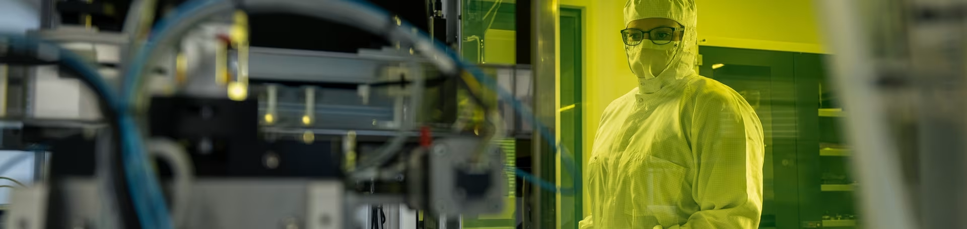
Do you work in a structured manner, are you reliable and ensure that our customers always receive the best possible support? Then join our team! In this position, you will be responsible for looking after and supporting our customers, providing training and ensuring that our machines and processes fulfil the high expectations of the Semiconductor Industry - all in a high-precision environment that also includes working in clean rooms.
At the earliest possible date we are looking for
Ihre Aufgaben
- Lead and drive the qualification, process development, trouble-shooting, characterization of advanced lithography processes for SUSS products to ensure competitive edge of processes performance for customer demands in the domain fields of advanced packaging for 2.5D/3D IC, CoWoS, CoPoS, FOWLP
- Improve the yield of process characteristics by analyzing process symptom data and performing for expertise documentation of technique to conduct lithography processes enhancement for sophisticated technical projects and events
- Act as the primary point of contact for on field key customers, manage multi-disciplinary projects and technical tasks of R&D or HVM from concept to completion, ensuring milestones on time and within planning scope
- Serve as subject mentor for junior colleagues to cultivate the continuous BKM techniques knowledge stewardship, accelerating the team's technical proficiency
- Take accountability and ownership of critical tasks and projects assigned by supervisor
Ihr Profil
- Education of Master or BS in engineering background for Physics, Optics, Material Science, Mechanical Engineering, Electrical Engineering
- 10+ years of proven experience in wafer fab working, specifically in lithography process engineering or field application
- Deep technical proficiency with lithography scanner and sophistic knowledge with 3D semiconductor or advanced packaging domains
- Analytical skills, self-motivated, resilience characteristics with good accountability
- Demonstrated experience in mentoring technical staffs and managing complex projects or tasks
Wir bieten unter anderem
- TW_We enrich your life with attractive rewards
- TW_Working hours that accommodate your individual needs
- TW_Working together and celebrating together
- TW_Your health is important to us