Senior Application Engineer - Scanner (m/f/d)
Onsite position – Kaohsiung/Tainan, Taiwan (local employment)
- Kaohsiung, Tainan
- Full-time
- Permanent
Big ideas often start small - sometimes smaller than a speck of dust. Microchips power the tools and devices we rely on every day - from smartphones and electric vehicles to medical diagnostics and AI systems. SUSS equipment enables their production through scalable, high-precision solutions in lithography, wafer bonding, and packaging. With over 75 years of experience and a global presence, we are a trusted partner that combines reliability and innovative strength.
We are guided by the conviction that innovation is not only created by technology, but by people who take responsibility and overcome boundaries together.
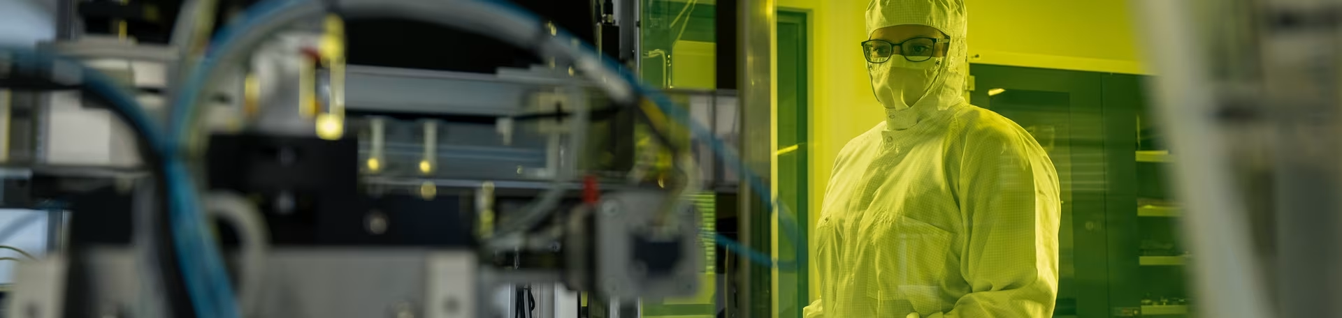
Do you work in a structured manner, are you reliable and ensure that our customers always receive the best possible support? Then join our team! In this position, you will be responsible for looking after and supporting our customers, providing training and ensuring that our machines and processes fulfil the high expectations of the Semiconductor Industry - all in a high-precision environment that also includes working in clean rooms.
At the earliest possible date we are looking for
Your Tasks
- Lead and drive the qualification, process development, trouble-shooting, characterization of advanced lithography processes for SUSS products to ensure competitive edge of processes performance for customer demands in the domain fields of advanced packaging for 2.5D/3D IC, CoWoS, CoPoS, FOWLP
- Improve the yield of process characteristics by analyzing process symptom data and performing for expertise documentation of technique to conduct lithography processes enhancement for sophisticated technical projects and events
- Act as the primary point of contact for on field key customers, manage multi-disciplinary projects and technical tasks of R&D or HVM from concept to completion, ensuring milestones on time and within planning scope
- Serve as subject mentor for junior colleagues to cultivate the continuous BKM techniques knowledge stewardship, accelerating the team's technical proficiency
- Take accountability and ownership of critical tasks and projects assigned by supervisor
Your Profile
- Education of Master or BS in engineering background for Physics, Optics, Material Science, Mechanical Engineering, Electrical Engineering
- 10+ years of proven experience in wafer fab working, specifically in lithography process engineering or field application
- Deep technical proficiency with lithography scanner and sophistic knowledge with 3D semiconductor or advanced packaging domains
- Analytical skills, self-motivated, resilience characteristics with good accountability
- Demonstrated experience in mentoring technical staffs and managing complex projects or tasks
We Offer Among Other Benefits
-
We enrich your life with attractive rewards:
NT$8,000 annual travel subsidy, NT$5,000 club activity subsidy, Birthday voucher & Mid-Autumn gift box, Quarterly team gatherings & Family Day events
-
Working hours that accommodate your individual needs:
10 days of annual leave from day one, 14 days of paid sick leave per year, leave above Labor Standards Act requirements
-
Working together and celebrating together:
Regular team-building events , family-friendly activities , supportive, people-first work culture
-
Your health is important to us:
NT$8,000 health check subsidy (every two years), NT$1,000 vaccination subsidy (age 40+), Pre-employment health check covered